Customer making a contactless card payment at a café counter using a modern POS terminal with transaction approved on screen

Payment Switch Development: Building the Core Engine of Payment Processing

This article explains the role of a payment switch at the center of every card and account-to-account flow and what it takes to build one that survives real production load. We walk through routing, authorization, message handling, integrations, security, and the engineering practices that separate a switch built to last from one that buckles under traffic.

Content authorBy EGSPublished onReading time14 min read

What a payment switch actually does

In payment transaction switching systems, a payment switch is the piece of software that sits between acquirers, issuers, card networks, and a bank's internal systems. Its job is to receive a transaction request from one party and pass it on in a form the next party understands after deciding what to do with it. Payment switch development is the discipline of building that middle layer so it stays fast and accurate with the availability production traffic requires.

The switch has three core jobs. First, real-time transaction routing: deciding the downstream path that should receive the transaction. Second, authorization: forwarding the request to the issuer (or standing in for the issuer when needed) and returning an approve or decline. Third, preparing the day's transactions for clearing and settlement so money actually moves between banks.

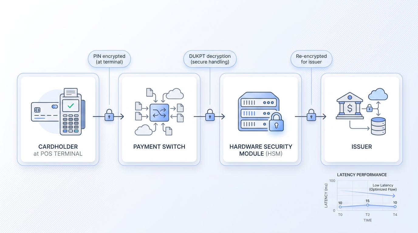
Here is the flow in plain terms. A customer taps a card at a coffee shop. The POS terminal builds an ISO 8583 authorization request and sends it to the acquirer. The acquirer's switch uses the card's Bank Identification Number (BIN) to identify Visa and route the message to the Visa network. Visa forwards it to the issuing bank's switch, which checks the balance and applies fraud rules before it replies with response code "00" for approved or "05" for declined. The response retraces the path back to the terminal. The entire round trip finishes in under two seconds.

Why the switch is the core engine

Every transaction in payment transaction switching systems passes through the switch. The mobile app, the POS, the e-commerce checkout, the core banking ledger, they all sit on one side or the other of it. That position is what makes the switch the real engine of payment processing, because every design decision inside it shows up in the customer's experience.

Latency is the clearest example. If the switch adds 200 milliseconds to each hop because of synchronous database calls or chatty logging, that delay reaches the terminal and the cardholder feels it. Reliability in payment switch development works the same way. When the switch drops a connection to the scheme, the front-end app has nothing useful to show. Cost per transaction also lives here, because real-time transaction routing choices made inside the switch determine which acquirer fees apply.

Front-end teams get the credit for a smooth checkout, but the switch is doing the work that makes the checkout possible. That is why banks and processors that take payments seriously invest in payment switch development as a long-term engineering capability.

Core capabilities of payment switch development

A switch that handles production traffic has to do several things well at the same time. The capabilities below are the ones that decide whether the platform holds up on Black Friday or falls over at 11 a.m. on a Tuesday.

Real-time transaction routing

Real-time transaction routing is how the switch decides where each message goes. The decision draws on the card's BIN range, the scheme (Visa, Mastercard, local network), the currency, the merchant category, the acquirer's contractual rules, and the cost of each available path. All of this happens in single-digit milliseconds because the customer is already waiting.

Most switches structure this as a combination of fast lookup tables for BIN and scheme data plus a rule engine for the business logic. Least-cost routing picks the cheapest acquirer that can settle a given transaction, which matters because interchange and scheme fees eat directly into margin. Fallback paths matter just as much. If the primary acquirer times out, the switch needs to retry through a secondary route without double-charging the cardholder.

When real-time transaction routing is done poorly, you see the symptoms in production: approval rates drop because traffic keeps hitting a degraded acquirer, and fees climb because the cheapest path is never selected.

Authorization and clearing flows

Payment transaction switching systems participate across the full lifecycle from the authorization request to the later clearing process, with capture handled along the way. Authorization is the real-time check that the funds and the card are good, signaled by a 0100 request and 0110 response in ISO 8583 terms. Capture happens when the merchant confirms the sale at end of day. Clearing is the batch process that produces the files banks exchange to actually move money.

Stand-in processing in payment switch development is the part that earns the switch its reputation. When the issuer is unreachable because of a network failure or maintenance window, the switch can approve low-risk transactions on the issuer's behalf using pre-agreed limits and a stored risk profile. The transaction completes, and the issuer reconciles later when it comes back online after the cardholder walks away with their coffee.

Reconciliation files tie all of this together. At cutoff, the switch produces settlement files that match every authorized transaction to its capture and clearing record. If these files do not balance, the operations team spends the next morning chasing breaks instead of working on anything productive.

ISO 8583 and ISO 20022 handling

ISO 8583 is the older standard and still the dominant one for card transactions. It uses a Message Type Indicator and a bitmap, with numbered data elements to encode everything from the card number (DE2) to the transaction amount (DE4) to the response code (DE39). It is compact, well understood, and ingrained in every card network.

ISO 20022 is the newer XML-based standard that carries richer structured data. Swift completed its cross-border migration to ISO 20022 on 22 November 2025, with 97% of payment instructions on the network already using the new format on day one. Further deadlines follow in November 2026, when unstructured messages and MT101 request-for-transfer support end.

Compatibility in modern payment switching systems

Modern payment transaction switching systems have to speak both. That means parsing each format and validating fields against the relevant scheme rules, while mappings between a card rail and an account-to-account rail preserve the richer ISO 20022 data without flattening it into something an old system can swallow. Vanesha Shurentheran of BPC Banking Technologies put the migration pressure this way: "Institutions that approach ISO 20022 purely as a compliance requirement will achieve minimal benefit; those that view it as a data foundation for operational and customer transformation will gain a long-term competitive edge."

The trap for existing switches in payment switch development is treating ISO 20022 as a bolt-on translator over an ISO 8583 core. That works until the day a regulator asks for the structured remittance data and your switch has already thrown it away.

Throughput and low latency

Payment transaction switching systems are measured in transactions per second. The global benchmarks set the ceiling: Visa averages around 8,500 TPS and can scale well above 65,000 TPS for peak events, while Mastercard reaches about 20,000 TPS at peak. Alipay hit 544,000 TPS during Singles' Day in 2019. National processors and large banks target somewhere between 1,000 and 10,000 TPS based on their footprint.

Latency budgets sit alongside throughput. A reasonable target for the switch's own processing time is under 50 milliseconds at the 99th percentile, which leaves room for network hops and the issuer's own response time within the two-second window the cardholder tolerates.

Hitting these numbers in payment switch development takes a specific set of engineering techniques:

  • In-memory caching of BIN tables and routing rules, plus recent transaction state so hot paths never touch disk

  • Asynchronous, non-blocking I/O so a single thread can hold thousands of open connections to schemes and acquirers

  • Horizontal scaling with stateless processing nodes behind a load balancer, with state pushed into shared stores like Redis or a distributed log

Load is measured before go-live. Realistic tests replay production-shaped traffic at 2x to 3x expected peak, with mixed message types and deliberate failure injection. Way4 Switch demonstrated 3,000 business TPS during a benchmark at Sun Microsystems in Langen, and that kind of structured benchmarking is what separates a switch you can trust from one you hope will hold.

24/7 uptime and failover

High availability for a switch is active-active deployment across at least two data centers and zero-downtime rolling upgrades, with geographic redundancy that survives the loss of an entire region. According to a Ponemon Institute study cited by Visa, one minute of downtime costs a business an average of $9,000, which puts an hour over $500,000. For a mid-sized acquirer, TNS estimates that a 30-minute outage processing 1,000 transactions per minute at $50 average value works out to $1.5 million in lost sales.

Failover behavior during a partial outage is where payment switch development designs are tested. If one node loses its connection to a scheme, the switch has to drain in-flight transactions cleanly and shift new traffic to healthy nodes after it marks the node as degraded, without producing duplicates. Hyperswitch, Juspay's open-source payments platform, targets 99.999% availability and up to 10K TPS, which translates to roughly five minutes of downtime per year as the design budget.

In-flight transactions are the hard case. A transaction that has been authorized at the scheme but not yet recorded locally needs a recovery path so it does not get double-presented or lost. That is why every serious design in payment transaction switching systems persists state at well-defined checkpoints and keeps an idempotency key on every message.

Integration with surrounding systems

Educational SaaS diagram illustrating a secure payment process from cardholder to issuer, with icons, arrows, and callouts in muted colors.

The switch never works alone. Its perceived speed and reliability depend on how well it talks to the systems around it.

Hardware Security Modules (HSMs) handle every cryptographic operation the switch needs. As Thales describes it, a payment HSM is a tamper-resistant device that protects cryptographic keys and customer PINs during card issuance and transaction processing. When a cardholder enters a PIN at a POS terminal, the PIN is encrypted at the device. Inside the HSM, a Derived Unique Key Per Transaction (DUKPT) scheme handles decryption before the PIN is re-encrypted under the issuer's key and forwarded. The switch never sees the PIN in clear, and the HSM round trip has to add as little latency as possible.

Fraud and core banking integration

Fraud engines plug in on the authorization path. The switch sends transaction features to the scoring engine and uses the returned risk score to approve or decline the transaction, with additional authentication as the step-up path. If the fraud call takes 300 milliseconds, the customer feels it. That is why most production setups run fraud scoring in parallel with other checks and apply strict timeouts.

Core banking integration is where the switch meets the ledger. For on-us transactions, the switch asks core banking for a balance check and posts the debit. Because the core banking system was designed for ledger work, the integration goes through a fast intermediate cache or a dedicated authorization service that talks to core banking asynchronously for posting. When integration in payment switch development is sloppy, customers see approved transactions that take hours to show up in their app, and that erodes trust faster than a decline would.

Security and compliance requirements

The baseline in payment switch development is non-negotiable. As of 31 March 2025, all formerly best-practice requirements in PCI DSS v4.0 became mandatory for any organization that stores or processes cardholder data, including those that transmit it. On top of that, every switch must hold current scheme certifications from Visa, Mastercard, and any local network it touches, and meet whatever the domestic regulator demands. Central banks across regions such as the Gulf and Southeast Asia have added their own audit and residency rules on top of the international baseline, with parts of Europe adding reporting requirements as well.

Key management is the part that punishes shortcuts. Master keys live inside the HSM and never leave it in clear. Working keys are rotated on schedules defined by the scheme and the regulator. Tokenization replaces the Primary Account Number with a surrogate value inside internal systems so that a leak of application logs does not expose card data. Audit logging records every administrative action and every transaction outcome in a tamper-evident store, because the auditor will ask for six months of evidence and "we deleted it" is not an answer.

Compliance is a continuous obligation. The certifications and standards change, and the scheme rules get updated several times a year. Treating the next audit as a project rather than a routine is how teams end up scrambling in March every year.

Common pitfalls in building a switch

Teams that try payment switch development in-house run into the same mistakes. They become visible only when production traffic finds them.

  1. Underestimating message format complexity. ISO 8583 looks simple in the specification and is anything but. Every scheme uses its own dialect, and private-use fields carry critical data that bitmap rules can hide from parsers tested only on textbook messages.

  2. Weak observability. A switch without per-message tracing and latency histograms per acquirer becomes a black box the moment something goes wrong; structured error logs need to be part of the same view. Operators end up guessing which leg of a transaction failed.

  3. Poor test coverage for edge cases. Reversals and partial approvals have to be tested as first-class flows, with late responses and stand-in scenarios included alongside timeout-during-capture in the same test plan.

  4. Skipping disaster recovery drills. A documented DR plan that has never been exercised is not a plan. Teams discover this when the primary region fails and real-time transaction routing reaches a secondary region with stale routing tables.

Each pitfall stays invisible during low-traffic pilots. They surface under load during the campaign or holiday weekend when the business can least afford an incident.

How EGS approaches switch engineering

EGS builds payment switches for banks and processors that need the platform to last a decade rather than a quarter. The starting point is domain-driven design: separating routing, authorization, clearing, and reconciliation into bounded contexts so each can evolve without dragging the others along. That separation in payment switch development is what makes it possible to swap a fraud engine or add a new scheme without rewriting the core. Performance work is done early and continuously. Every release goes through automated load tests that replay production-shaped traffic at multiples of current peak, with synthetic failures injected to confirm that failover behaves as designed. The team measures latency at the 99th and 99.9th percentile because averages hide the cases that actually hurt customers.

Rollouts are phased. A new switch or a major change goes live for a single corridor or a single product line first and runs in parallel with the existing system so results can be compared transaction by transaction; it only takes full traffic once the numbers match. This is how Cognizant describes migrating logical chunks of functionality while maintaining a host-ISO bridge between old and new, and it is the approach that keeps the bank's customers from becoming the test population. The switch is treated as a long-term platform. That means investing in observability, in runbooks, in clear interfaces to surrounding systems, and in the engineering team that owns the platform after go-live. A switch handed over without that ownership becomes a liability within two years.

Planning your next step

A payment switch is worth the investment when transaction volume or regulatory exposure outgrows what an off-the-shelf product can absorb, especially when product ambition also exceeds it. The signals are familiar: rising fees that nobody can explain and outages that cost more than the platform itself, especially when schemes ask for changes the current vendor cannot deliver. When those signs show up together, it is time to look seriously at payment switch development.

EGS works with banks and processors on payment switch development as resilient fintech infrastructure, from greenfield builds to replacing legacy switches that have run their course. If you are weighing whether to extend or replace, talk to our team for a focused assessment of your current setup and a plan for what comes next.

Payment switch development usually takes months, not weeks, because certification, testing, and integrations drive the timeline. A narrow first release with one scheme and one product line is faster than a full replacement. Teams should plan time for ISO testing, HSM setup, failover drills, and scheme approval.

A payment switch should log the message type, route, response code, timestamps, correlation ID, and final state for each transaction. It should avoid storing sensitive card data in plain form. These logs help operations teams trace failed authorizations, prove audit history, and reconcile settlement breaks.

A bank can run a payment switch in the cloud if regulation, scheme rules, latency, and key management requirements allow it. The design still needs HSM integration, network isolation, active-active deployment, and tested recovery steps. Data residency rules often decide which cloud region or hybrid model is acceptable.

You should replace an existing switch when outages, certification delays, high operating costs, or missing features block business goals. Extension makes sense when the core is stable and only a limited module needs work. A replacement is safer when routing, observability, or message handling can’t support planned volume.

EGS can assess the current switch, identify failure points, and plan a phased modernization path. As a provider of resilient fintech infrastructure solutions, EGS works on routing, authorization, clearing, reconciliation, and production readiness. The goal is to reduce migration risk while keeping payment traffic measurable during each rollout stage.

Schedule a Meeting

Book a time that works best for you

You Might Also Like

Discover more insights and articles

Title:
Instant Debit Cards: Enabling Immediate Payment Access

Meta description:
Learn how instant debit cards let you spend funds moments after account approval. Read this guide to understand the dig

Instant Debit Cards: Enabling Immediate Payment Access

In this article, we explain what instant debit cards are and how the technology lets customers spend within seconds of opening an account. We walk through the customer flow, the benefits for both sides of the transaction, the security behind it, and where the technology is heading.

Title:
Virtual Card Issuing: Secure Digital Payments for Modern Fintechs

Meta description:
Learn how virtual card issuing works so you can select the best provider and launch secure payment features.

Virtual Card Issuing: Secure Digital Payments for Modern Fintechs

This article explains how virtual card issuing works under the hood and why it has become a core building block for fintech products. It walks through the infrastructure, common use cases, security obligations, and the criteria that matter when picking a provider.

Title:
White Label Card Issuing: When to Use It and When to Build Your Own

Meta description:
Decide if white label card issuing fits your business or if you should build your own stack. Learn the tra

White Label Card Issuing: When to Use It and When to Build Your Own

This article explains how white label card issuing works and helps fintech founders and product leaders decide whether to license a ready-made platform or build their own stack. It covers the trade-offs and what to verify before signing anything.

Title:
Card Issuing Platform: Architecture for Scalable and Secure Card Programs

Meta description:
With a modern card issuing platform, you can scale your program safely. Learn to design a secure arc

Card Issuing Platform: Architecture for Scalable and Secure Card Programs

This article walks fintech leaders and product-engineering teams through the architectural layers behind a modern card issuing platform. We break down the stack from the issuing processor to the API gateway, then show how the pieces cooperate during a live authorization before the article closes with a checklist for evaluating any vendor or in-house build.