Hardware abstraction layers
In embedded POS software, a hardware abstraction layer (HAL) sits between your payment logic and the device-specific SDKs and silicon underneath. Done well, the same core application moves to new hardware with far less rework, because a stable interface isolates the hardware-specific paths behind a boundary.
The payoff is the part a product leader weighs. A clean HAL reduces vendor lock-in and makes hardware transitions manageable as deployments grow. It also speeds re-certification when the hardware changes. That last point isn't small. PCI PTS change-control rules force re-certification on security-relevant hardware changes, so the less your payment core has to change when the silicon does, the less of that cycle you repeat.
There's a tension to manage, though. A HAL that abstracts cleanly can also add overhead the constrained CPU and memory can't absorb. Every layer of indirection costs cycles, and cycles are what you're rationing inside a sub-second transaction window. For embedded payment systems, the architecture has to abstract enough to be portable without inserting itself into the hot path of a tap or a dip. Get that balance wrong and you've traded portability for missed timing windows, which is the worst trade in this business.
How certification reshapes development cycles
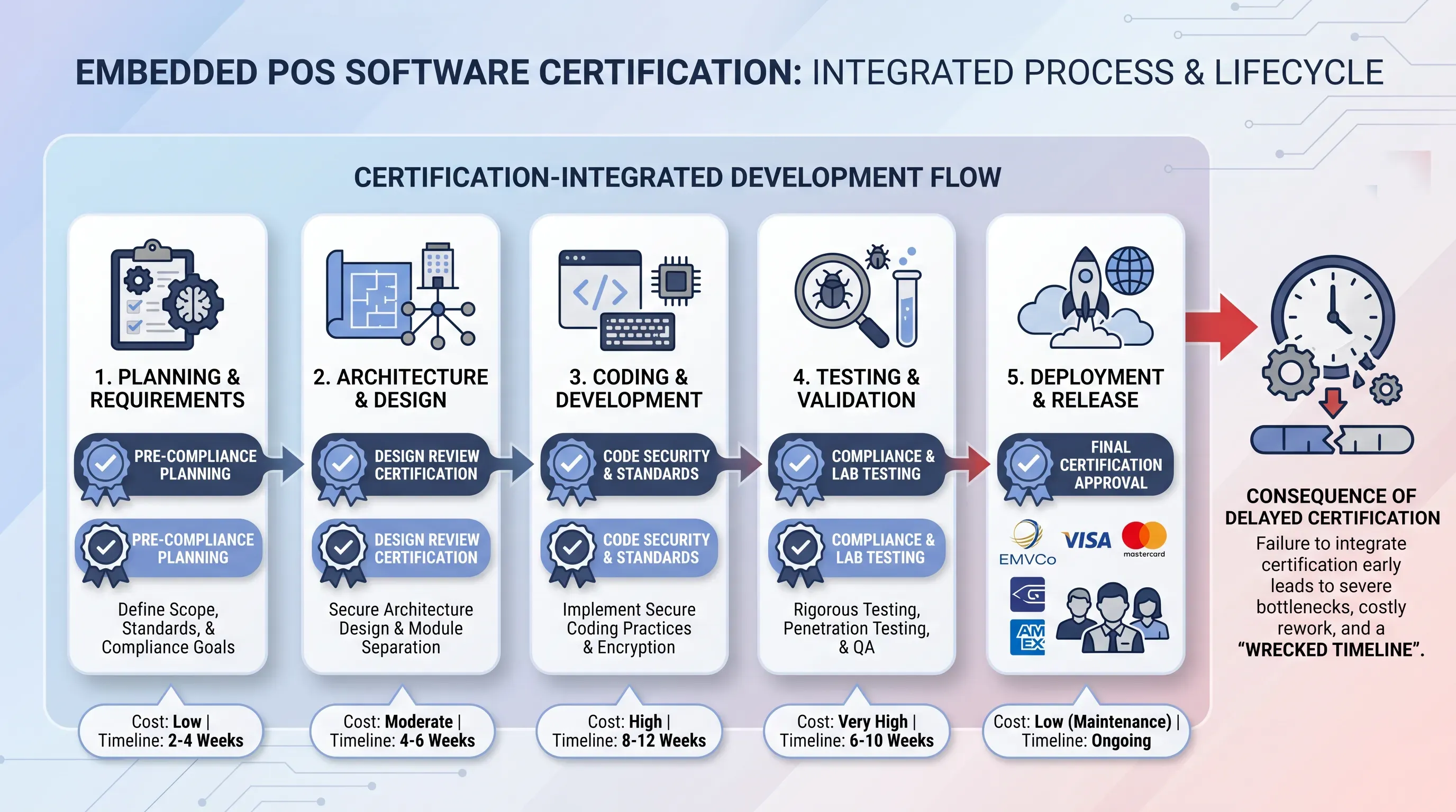
The instinct is to treat certification as a final gate, a test phase you schedule at the end. That instinct is what wrecks timelines. For embedded pos software, certification shapes the whole project, and it does so from the first architectural decision.
For embedded payment systems, four distinct approvals are in play, and they don't overlap neatly:
Levels 1 and 2 are certified by EMVCo, but Level 3 has to pass tests with each card brand individually, so each card brand demands its own approval. That single fact multiplies the work. A custom payment application is held to the same testing standard as a generic one, and the burden falls on whoever wrote it.
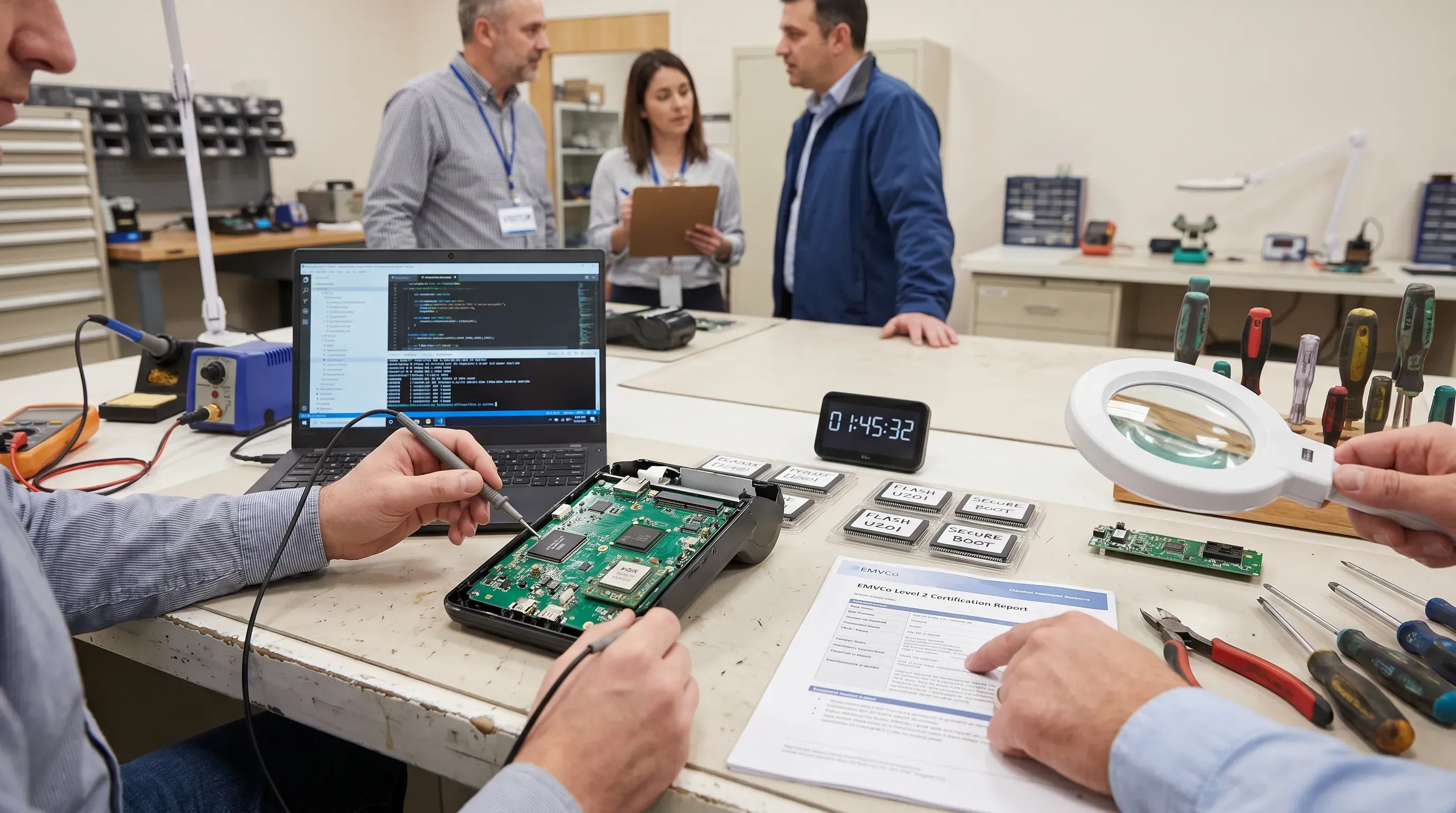
Now the schedule reality. A single terminal model's Level 3 network certification in the U.S. "can take a few months and cost thousands of dollars," and that's per terminal per network. Blankfactor notes the full path "can take up to two years or maybe more." Worse, it repeats. Firmware and software updates in pos firmware development require portions of the L3 certification process to be repeated, so every meaningful change reopens part of the cycle. Mature teams design for certification from day one, with test planning and host simulation built into the architecture before lab work exposes any gaps.
Why most vendors cannot do both
The biggest challenge in embedded POS software is bringing together two specialized disciplines: low-level embedded engineering and payment certification. Teams often excel at one but lack the other, leading to delays, redesigns, or certification hurdles late in the project.
Successful delivery requires expertise across firmware, EMV kernels, PCI requirements, and certification from the start. As the U.S. Payments Forum, quoted by Blankfactor, notes, certification timelines are often extended by testing, scheduling, and review cycles that experienced teams know how to plan for.
At EGS, we combine embedded engineering with end-to-end payment integration and certification expertise, covering firmware, kernel integration, and key management as one coordinated effort. If you're planning or scaling an embedded POS software project, reach out to discuss your requirements and the most practical path to certification.